Hardware Documentation and Howto's: Difference between revisions
From pCT
No edit summary |
mNo edit summary |
||
| (39 intermediate revisions by 3 users not shown) | |||
| Line 1: | Line 1: | ||
[[Main Page]] -> [[Hardware Documentation and Howto's]] | |||
== Getting Started == | == Getting Started == | ||
| Line 8: | Line 10: | ||
=== pRU === | === pRU === | ||
* [[:Media: | * [[:Media:Clock_network.png | pRU Clock Network]] | ||
* [[:Media:PRU Address Map.pdf | pRU Address Map]] | * [[:Media:PRU Address Map.pdf | pRU Address Map]] | ||
* [[:Media:PRU Ethernet Configurations.pdf | | * [[:Media:PRU Ethernet Configurations.pdf | DCS and Data Offload Ethernet Configurations]] | ||
* [[:Media:PDTP.pdf | pCT Data Transfer Protocol]] | |||
* [[:Media:Data format v0.2.pdf | pRU Data Format]] | * [[:Media:Data format v0.2.pdf | pRU Data Format]] | ||
* [[:Media:FpgaCalc.ods | FPGA and ALPIDE radiation calculations]] | |||
* [[:Media:Control Interface.pdf | pRU Control Interface]] [Deprecated, only in use on PTB. Replaced with IPBus on VCU118 + all other boards in the future.] | |||
==== pRU Registers and Bus System ==== | |||
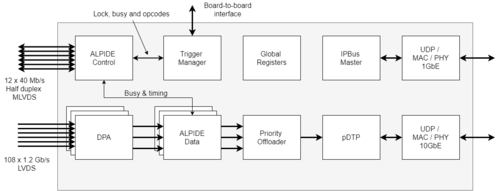
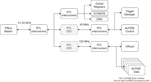
[[File:Top level firmware.png|500px]][[File:Bus tree.png|500px]] | |||
The pRU bus system is connecting the various modules on the FPGA to a common master, the Microblaze Subsystem. | The pRU bus system is connecting the various modules on the FPGA to a common master, the Microblaze Subsystem. | ||
Each of the modules is associated with a given BASE-ADDRESS specified in the [[:Media:Control Interface.pdf | pRU Control Interface Document]]. | Each of the modules is associated with a given BASE-ADDRESS specified in the [[:Media:Control Interface.pdf | pRU Control Interface Document]]. | ||
| Line 24: | Line 30: | ||
* 1st instance: <ALPIDE_DATA_BASEADDR> | * 1st instance: <ALPIDE_DATA_BASEADDR> | ||
* 2nd instance: <ALPIDE_DATA_BASEADDR> + (0x1000 * 2-1) | * 2nd instance: <ALPIDE_DATA_BASEADDR> + (0x1000 * (2-1)) | ||
* 16th instance: <ALPIDE_DATA_BASEADDR> + (0x1000 * 16-1) | * 16th instance: <ALPIDE_DATA_BASEADDR> + (0x1000 * (16-1)) | ||
=== | ===== Module Registers ===== | ||
* [[:Media:Global_regs.pdf | global_regs]] | |||
* [[:Media:Trigger_manager.pdf | trigger_manager]] | |||
* [[:Media:Offload.pdf | offload]] | |||
* [[:Media:Alpide_control.pdf | alpide_control]] | |||
* [[:Media:Alpide_data.pdf | alpide_data]] | |||
==== PTB-specific Module Registers ==== | |||
* [[:Media:Power_control.pdf | power_control]] | |||
* [[:Media:Ptb_regs.pdf | ptb_regs]] | |||
=== Transition Card (TC) === | |||
* [[Media:TC-v1.0_schematic.pdf | TC-v1.0 Schematic]] | |||
=== ALPIDE Chip === | |||
* [[Media:Alpide manual ver3.pdf | ALPIDE Manual v0.3]] | |||
=== ALPIDE Bonding and Mounting === | === ALPIDE Bonding and Mounting === | ||
* [[:Media:Report_Feb_2019.pdf | 9-chip String Simulation - and proposed 9-chip string redesign - 2019 Feb ]] | |||
==== Chip Cable ==== | ==== Chip Cable ==== | ||
* [[:Media:2020_01_08.zip | 2020 January 8 ]] | |||
* [[:Media:2019_05_16.zip | 2019 May 16 (ULTM)]] | |||
==== 9 Chip String ==== | ==== 9 Chip String ==== | ||
* [[:Media:2019_11_05.zip | 2019 November 5 ]] | |||
* Some of the aluminium traces on the flex cable broke by the tail of the cable (near the ZIF stiffener). [[Media:Tail_modifications.png | Current design and possible modifications]] shows the current design and two possible modifications. It has been decided that new designs will use the '''design 1 modification''' and '''longer ZIF-stiffener''' (30 mm long). | |||
=== Production Test Box (PTB) === | |||
* [[:Media:PTB-v1.0_schematic.pdf | PTB-v1.0 Schematic]] | |||
* [[:Media:PTB-v1.0_samtec.zip | PTB-v1.0 FPGA Connections]] | |||
* [[:Media:PTB-v1.0_yamaichi.zip | PTB-v1.0 Yamaichi Connections]] | |||
=== FPGA Mezzanine Card (FMC) === | |||
* [[:Media:FMC-v1.0_schematic.pdf | FMC-v1.0 Schematic]] | |||
=== mTower === | |||
* [[:Media:mTower_schematic.pdf | mTower Schematic]] | |||
Latest revision as of 11:43, 23 August 2023
Main Page -> Hardware Documentation and Howto's
Getting Started
Documentation
pRU
- pRU Clock Network
- pRU Address Map
- DCS and Data Offload Ethernet Configurations
- pCT Data Transfer Protocol
- pRU Data Format
- FPGA and ALPIDE radiation calculations
- pRU Control Interface [Deprecated, only in use on PTB. Replaced with IPBus on VCU118 + all other boards in the future.]
pRU Registers and Bus System
The pRU bus system is connecting the various modules on the FPGA to a common master, the Microblaze Subsystem. Each of the modules is associated with a given BASE-ADDRESS specified in the pRU Control Interface Document. Note that several instances do exist for certain modules. E.g. there are one alpide_data instance for each ALPIDE chip connected to the pRU. To communicate with a specific instance one needs to add an offset of 0x1000 times the instance number to the module base address.
E.g. if you want to communicate with the
- 1st instance: <ALPIDE_DATA_BASEADDR>
- 2nd instance: <ALPIDE_DATA_BASEADDR> + (0x1000 * (2-1))
- 16th instance: <ALPIDE_DATA_BASEADDR> + (0x1000 * (16-1))
Module Registers
PTB-specific Module Registers
Transition Card (TC)
ALPIDE Chip
ALPIDE Bonding and Mounting
Chip Cable
9 Chip String
- 2019 November 5
- Some of the aluminium traces on the flex cable broke by the tail of the cable (near the ZIF stiffener). Current design and possible modifications shows the current design and two possible modifications. It has been decided that new designs will use the design 1 modification and longer ZIF-stiffener (30 mm long).


